2009年11月18日 星期三

Three Band Tone Control


FEATURES

1. Support 3 bands (bass, mid and treble frequency) tone control for stereo channel. Frequency range is turnable by three variable resistors.
2. Use of very low distortion high quality audio opamp TDA2320A, 0.03% at f=1kHz typical 3. High power rejection ratio: 80dB and channels isolation: 100dB
4. Symmetric PCB design for both R and L channels.
5. Implemented with WIMA, nichicon capacitors and Dale resistors.
6. High quality PCB, blue solder mask, double layer, 2.4mm thickness, 2oz copper.
7. Required power supply: +/-15V DC

8. Dimension: 141mm x 56.4mm


ASSEMBLY GUIDE

1. Solder all the components according to the part list which can be downloaded from this forum.
2. Unplugged the ICs before applying +15V and -15V DC supply.
3. Plug back the ICs if there is no abnormal large current drawing from the supply.


TEST RESULTS
Yellow trace show the input signal
Blue trace show the output signal

Attenuation for frequency at 100Hz, 1kHz, and 10kHz


Yellow trace show the input signal
Blue trace show the output signal


Gainfor frequency at 100Hz, 1kHz, and 10kHz


2009年11月17日 星期二

Timing Control DIY


FEATURE

1. Timing Adjustable relay switches from mili-seconds to hours.
2. Time setting by varies RC value of the 555 Timer.
3. Built-in low dropout voltage regulator LM1086-5 IC.
4. Wide range of DC Power supply: 6-30V
5. Max rating of Relay: 120VAC 1A

Applications: Delay protection for speaker, power supply, etc.


ASSEMBLY GUIDE
1. Soldering the components according to the schematic and BOM.
2. The timing constant (delay time) is set by the RC time constant, that are the resistors R1, R2, R3, R4, R5, and R6, and C4. The higher the time constant, the longer delay time will be resulted. The relationship between the delay time ranged from micro seconds to few seconds is shown in the below figure. By properly setting the RC value, you can control the delay time of the relay switch.
3. Apply the power supply, you will hear the 'click' sound or LED light up when the relay are switched on after the predefined delay timing.


2009年11月15日 星期日

Citation 12 MOSFET Power Amplifier


FEATURES
1. Design reference to the Harman-Kardon Citation 12 classic power amplifier circuit as blueprint and circuit modified as reference to Nelson Pass
2. Maximum output power can reach 75W for 8 ohm output loading
3. High precise MOSEFT IRFP240
4. Built-in voltage regulating circuitry, come with Nichicon Muse for power filtering capacitor
5. This kit use WIMA 0.1uF/400V as bypassing capacitor and Dale resistors
6. PCB dimension: 10mmx14mm, 2.5mm thickness and 2oz copper

Optional: Toroid Transformer T200 200W (for two channels)


ASSEMBLY GUIDE
1. Assembly all the components according to the schematic and part list (which can be downloaded in this page)
2. Open the bypass jumper J3, J4, J12 and J13 before switch on power.
3. Apply two 27V AC to J1 and J2. ~33V DC is obtained for the filtering capacitor C1, C3, C5, C7, C9 and C11 and ~-33V DC is obtained fo the capacitors C2, C4, C6, C8, C10 and C12. This step is to ensure the power supply block work well.
4. Remove the power supply and discharge the capacitors (short by a 10ohm/2W resistor to ground). Open the bypass jumper J3 and J4 and short the J12 and J13 by wires, power supply is now in series with the 10ohm/2W resistor to limit its maximum current supply to the circuit in case of any components burnt out (This step important!). Also, large heat sink is required to drain out the heat generated by two power MOSFET. The MOSFET is very hot, dont use figure to touch it!
5. The R16 and R21 is used to measure the biasing current of the output stage (high biasing current mean high output driving current and hence higher output power). At the beginning, the resistor trimmer RV1 is set so that the biasing current is as small as possible to prevent burnt out of MOSFETs due to high current (turn it until it reach the most anti-clockwise position)
6. Turn on the power supply. Disconnect the power supply when you see any smokes, lighting or smell any burnt. Ensure the resistor trimmer is set in the correct position.
7. Measure the voltage across the 10/2W resistors (J3 and J4), the biasing current can be calculated by the following equation:
I = V/ R = V/10
Gradually turning the resistor trimmer VR1 until the biasing current I reach to 75mA - 100mA (V=1V). Again, higher biasing current, higher output power, but I=75mA is suggested. (Disconnect the power supply if see there is any smokes)
8. Short J3, J4, J12 and J13 by wires। Everything is finished and enjoy it!


(Input / Output) Channel Selector (Relay & LED)


FEATURE
1. Support 4 audio inputs (RCA) and 1 balanced input (XLR) for both R and L channels .
2. Blue/White LEDs for indicator.
3. Built-in voltage regulator.
4. Required DC supply voltage 8-13V, and which can be supplied by tube amp.
5. PCB Dimension: 120mm(L) x 53mm(W)


ASSEMBLY GUIDE
1. Soldering the components according to the schematic and BOM.
2. For the 5 pin white connector, label 'E' is GND pin, whereas 'D', 'C', 'B', 'A' are the control pins for channel 1, 2, 3, and 4, respectively.
3. Apply 9-15V DC to the power supply connector, the LED will be led on while the corresponding control pin ('A', 'B', 'C', and 'D') is connected to 'E', that is grounded the control pin.


Dale 23 Steps Attenuator


OVERVIEW

1. Dale resistors, 23 step attenuator and knob.
2. Ladder type structure, 23 sections.
3. Log scale attenuation.
4. Rotary are Made-before-break

The DIY Kit come with a resistor pack, 23 step rotary, and aluminum knob. The available values are 10k, 50k, 100k, and 250k ohm.


ASSEMBLY GUIDE
The circuit diagram displays the configuration of the serial resistor network (ladder type) which consists of Rin and Rg. For one channel, there are 23 pair of Rin and Rg. The total equivalent resistance R=Rin + Rg, this value are fixed, so that the input resistance is more or less the same (ideally we want it to be constant)


Procedures to assembly:
1. Identify the resistor values (Rin and Rg) for two channels according to the following resistor list (10k, 50k, 100k and 250k). You could paste the resistors by plastic tapes on a paper one by one, where the number of 1 to 23 are marked.
2. Locate the postion 1, 2, 3, ..., 23 position of channel 1 and channel 2.
3. Solder the resistors Rin and then Rg.
4. Connect the GND, signal in, and signal out.
5. Finally, test it and good luck.


The complete one should look like (but the wire colors maybe different in different cases):


The resistor list for 10k (the resistor values started by position 1 and till to position 23):

The resistor list for 50k (the resistor values started by position 1 and till to position 23):


The resistor list for 100k (the resistor values started by position 1 and till to position 23):


The resistor list for 250k (the resistor values started by position 1 and till to position 23):

Variable Tube Power Regulator 190V-450V


FEATURE

190-380V or
250-450V
DC (100mA) for tube preamplifier
0-15V DC (1.5A) x2 for tube filaments / other applications
1. Adjustable tube power supply by resistor trimmer for tube preamplifier, for examples, Jadis JP-200, Cary AE-ONE, Marantz 7, etc.
2. Incorporating flexible design: Use 5Z2/5Z3/5U4/6X4/Two diodes as rectifer, EL84/6P14 as voltage regulating tube and EF86/6J8 as buffer tube
3. Additional power supply for filament: adjust to 6.3V/12.6V (1.5A) x2
4. Double blue layer PCB, 250mmx120mm, PCB thickness of 2.5mm, 2 oz copper metal, come with schematic.
5. Socket provided for filtering choke 10H 150mA connection or manually short.


ASSEMBLY GUIDE
1. Soldering the components according to the schematic and part list which can be downloaded from here.

2. For 190-380V DC output, D1 uses
1N5378B
For 250-450V DC output, D1 uses 1N5383B
3. Connect the power transformer according to the schematic and switch on the power supply
(turn it off if found any smokes from transformer or the tubes does not light up properly).
4. Measure the voltage across the J4
(Dangerous! Be care of high voltage!), J6 and J7. The voltage of J4 will be gradually increase until reach preset voltage.
5. Output voltage can be adjusted by VR1.

Ensure all high voltage capacitors are fully discharged after switched off the power supply! (it normally takes few minutes)


High Power BJT Regulator DC 50-400V


Features
1. High voltage output voltage: 50V - 400V DC up to 100mA
2. Low voltage output voltage: 0-30V up to 5A
3. High power BJT switch E13005 and regulators LM1085 and LM1084
4. Output voltages can be adjusted by two resistor trimmers
5. Three BHC audio capacitor 100uF/450V and WIMA 100nF/450V for high voltage decoupling capacitors.
6. Two BHC audio capacitor 10000uF/63V for low voltage ripple decoupling capacitors.
7. Dedicated ground and power rails layout design
8. Lowpass filter with optional inductor 10H 100mA.
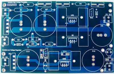
9. PCB dimension: 154mm x 98mm


Required power supply:
For HV regulator: 200/220/240/260/280/300V AC / 100mA
For LV regulator: 12/15/18V AC / 1-5A

Optional T30 toroidal transformer:


Schematic and Layout
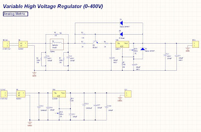


ASSEMBLY GUIDE
Precaution:
1. Do not use any body parts to touch the metal parts of the kit after power up or power off, since the high voltage capacitors may not fully discharge. It may cause serious electric shock.
2. Use a power transformer with fuse (1-3A) socket to limit the supply current in case of short circuit or incorrect assembly.
3. Double check the assembled components with the schematics.
4. Do not attempt the measure the voltage by multimeter with hand after power up. The probes of the multimeter should be mounted by some stands to the points of the measurement before switching on the power supply.
5. Turn off the power supply if you observe any smokes or hear strange sound coming out from the transformer or board. If there is short circuit, the transformer will be getting very hot shortly.

Procedures.
1. Solder all the resistors and two blue resistor trimmers 1k (102) and 5k(502) according to the schematic and part list. The biggest resistor is 5W, whereas smaller one is 2W.
2. Solder two diodes 1N4007 and Zener diode (1N4733A). Notice the direction of the diodes and Zener diode. There are white bar marked in board corresponding to the bar of the components. The Zener diode looks similar to the silicon diode (standard diode). However, their operation direction of current flow is totally different. The Zener diode is slightly smaller than the diodes. In the photo, the Zener diode is displayed as orange in color with dark line.
3. Mount the power BJT M13005, regulators LM1085/LT1085 and LM1084 to the heat sinks by the provide screws and nuts. Their packages are idential, however do not mix up the BJT with the regulators. It will cause the voltage breakdown of the regulator.
4. Solder the high voltage capacitors 100uF/450V and low voltage capacitors 10000uF/63V. Be care of the polarity of the capacitors. There have a "+" marked in PCB for indicating the positive pin.
5. Solder the remaining components.
6. Connect optional inductor 10H 100mA for further attenuation of the the ripply voltage or leave it unconnected.
6. Apply 200/220/240/260/280/300V AC to the connector (Blue) to the high voltage regulator and 12/15/18/24/27V AC to the connector (Blue) of the low voltage regulator as shown in the below photo.
7. For higher output voltage, apply higher AC voltage to the board. For example, 300V AC to produce output voltage 100-400V or 220V AC to produce output voltage in range from 50- 280V DC. To allow high efficiency of the regulator, the difference between the output voltage to input voltage should be small. Otherwise, much of input power will be dissipated in form of heat.
8. For high voltage module, the output current is limited by the resistor R1 (1K ohm 5W). To increase the output current, the resistor R1 should be decrease. The recommended range is 10-1K Ohm.


Checklist:
1. The direction of diodes and Zener diodes.
2. The polarity of the high voltage capacitors.
3. The correct assembling of diodes, Zener diodes, high voltage capacitor, power BJT and regulators.